
- HOME
- About HOLON
- Business of HOLON
HOLON’S Philosophy
HOLON measures the invisible small world
with a nanometer scale

The term HOLON was created by the Hungarian-born philosopher Arthur Koestler. It originates from the Greek word "holos" for whole, with the suffix "on" attached, which signifies a piece or a part. The meaning of this word relates to the organic harmony in the relationship between the individual and the group, or the individual and the whole. In other words, the larger the scale of observation, the more an object will emerge as part of the total, and the smaller the scale of observation the greater the number of structural constituents, thus depicting a contained whole with a certain property of containment.
HOLON proposes to contribute to the furtherance of society by bringing out the full potential of every employee and letting employees achieve success by converging in an organic and harmonious manner on the creation of manufactured products.
Business of HOLON
Business of HOLON is manufacturing measurement tools for ascertaining the design-conforming, correct production of semiconductors, which are indispensable for devices such as PCs, smartphones, and digital home appliances with their ever-smaller dimensions and relentlessly advancing functions and performance attributes.
These days, it is known that EUV lithography is being implemented for high volume device production of leading-edge technologies. Our Defect Review SEM (DR-SEM) has become an indispensable tool in this area.
In order to fulfill this particular role in the rapidly evolving semiconductors and nanotechnology industries, HOLON has been striving to strengthen cooperative partnerships in research and development, manufacturing and marketing, and equipment preservation and maintenance, and will continue to provide optimal services.
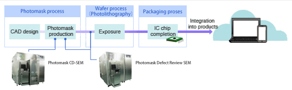
What is a CD-SEM?
SEM is short for Scanning Electron Microscope. Electron beams are directed against a sample surface, an image of the test material surface is obtained by detecting the secondary electrons emitted from it in response. A CD-SEM is a Critical Dimension SEM, a tool that uses SEM technology in order to measure pattern dimensions. The Z Series, a main product of HOLON, is a CD-SEM for measuring the patterns of masks for semiconductor fabrication.
What is a DR-SEM?
A DR-SEM (Defect Review Scanning Electron Microscope) provides high resolution images of any defects located by mask tools, allowing the defects to be viewed and classified. This is especially important for EUV masks that have very challenging defect specifications. The DR-SEM also indicates the chemical elements found in the defects, assisting in the investigation and elimination of their source to improve mask yield.
HOLON’s DR-SEM is based on the same technology platform as the CD-SEM.