

Photomask CD-SEM
HSS-1000
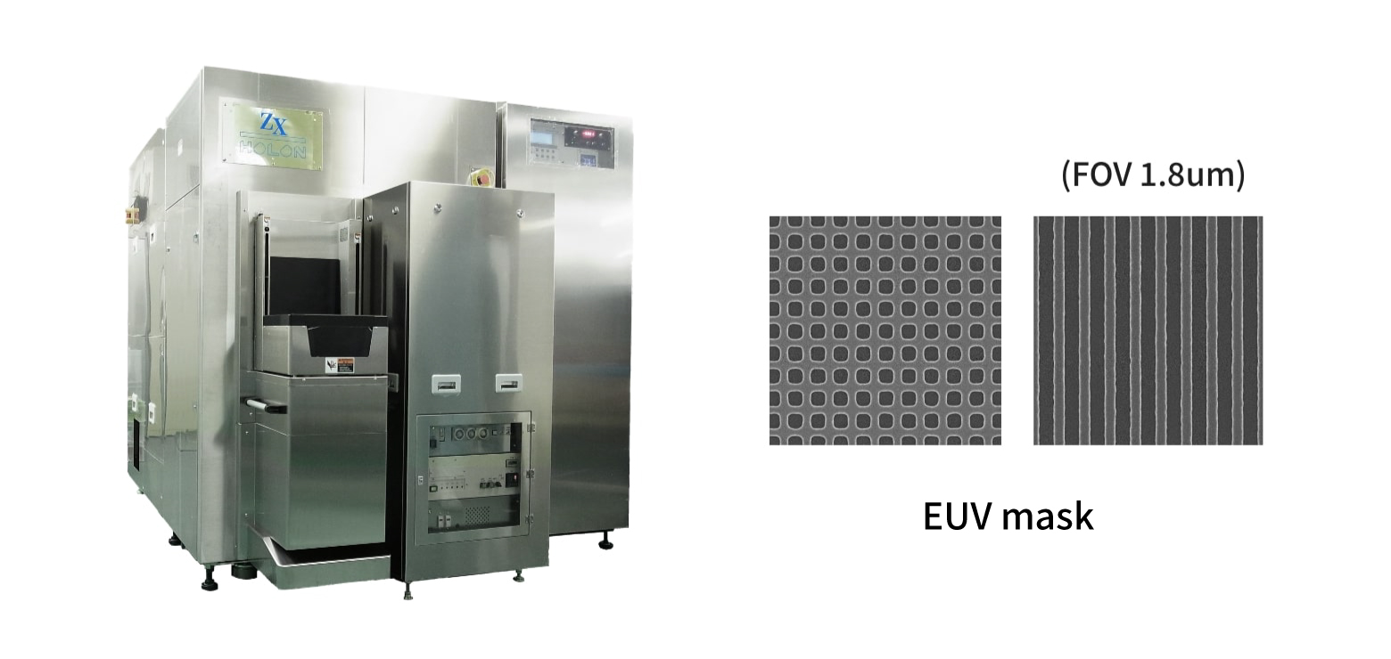
HSS-1000 offers significantly improved performance over the previous ZX model, achieving the extremely high CD measurement accuracy required for EUV mask manufacturing in the 1.6nm node and beyond. Furthermore, it is capable of acquiring clear, high-resolution SEM images of thin-film absorber layers and photoresist patterns.
Main Features
- - Newly designed electron optical systems and aberration correction technology enable high-resolution SEM images and significantly improves measurement accuracy of fine patterns.
- - The beam control circuit has the same accuracy and speed as ones for an EB lithography system, which enables high-speed and high-precision CD measurement, strengthening its capabilities in mass production use.
- - Low incident energy (100 eV) allows for low damage to photoresist patterns, enabling high-resolution measurement while suppressing resist shrinkage
- - The newly designed platform's pallet-less transport and high-speed stage significantly improve throughput, meeting the needs for mass production.
- - AI technology predicts and corrects for focus and positioning deviations of the e-beam, and De-noise processing enables higher resolution and stabilization of SEM images.
- - Implementation of low vacuum technology and VUV provides powerful charging-mitigation solutions to suppress image degradation caused by charging effect and support stable measurement.
- - High-precision contour extraction function enables EPE analysis for curvilinear patterns.

ZX
The ZX CD-SEM extends HOLON’s technical leadership in mask metrology to the most advanced devices at sub-10nm nodes.
HOLON’s industry-leading Aberration Correction and Charge Mitigation technologies have been refined and implemented to address all the requirements for measuring and imaging leading-edge semiconductor photomasks.
The ZX has been delivered to and is used at multiple semiconductor manufacturers, foundries, and photomask shops around the world.
Features
- - High-speed and high-precision measurement of patterns on the nanometer scale
- - Improved Aberration Correction for sharper images with higher signal-to-noise ratio
- - Charge-mitigated High Quality Images enabled by Low Vacuum Technology
- - Integrated applications including Multi-point CD Measurement, Contour Extraction, New 2D Measurement, Method, Defect review, and “Bird’s Eye” (3D) View
- - Applicable for various substrates including EUV masks, phase shifting masks, NIL Qz Molds, PET Film Molds, and DSA Films
ZX-D
ZX-D is a photomask CD-SEM for legacy process nodes.
The ZX-D and ZX are built on the same technology platform, and the ZX-D can be upgraded to the full ZX configuration when needed.
※Please click here for additional product information.